1.6 create AOI device PCB thumbnail and offline diagram
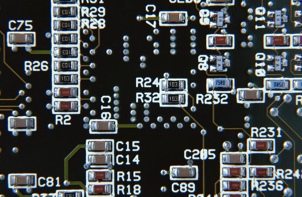
The thumbnail is a miniaturized image of PCB tested by AOI equipment, which is convenient for global observation, display of error position and other related operations. At the same time, if you want the lens to move to a certain position, you just need to double-click the corresponding position on the thumbnail.
Production method: after completing the operation of the menu bar of the new program, click OK, and the system will automatically prompt "do you want to make PCB sketch now?" Click "yes", and the system will scan the PCB thumbnail according to the set PCB calculation starting point and size. Or directly click "make panel drawing" in the lower right corner of the main window, as shown in the figure below:
In order to enable the thumbnail to display PCB completely, the appropriate reduction ratio can be selected. Generally, it is appropriate to display the outline image of the whole PCB in the thumbnail window. Click "full picture" to automatically expand and expand the PCB thumbnail according to the screen size of the window, so as to achieve the best display effect of the thumbnail. The way to make an offline AOI device diagram is similar to that of making a thumbnail (just select the location and file name to save the image). The off-line AOI device diagram can be used on other computers (other than the computer on this device) to compile test program (the use mode is similar to that of the equipment).

Note: the offline AOI device is programmed as an option function. If necessary, please purchase it separately.
1.7 set mark point
Generally, two easily recognized points are selected as mark points in the diagonal position of PCB, which can be mark points existing on PCB itself, or holes with fixed position on the board as mark points.
Note: 1. When the mark point on PCB is often oxidized, try to use the upper hole position as mark point. Because Yier AOI equipment is sensitive to color change, a little change may lead to mark recognition error, and the color change of hole position is generally smaller. (as shown in Figure 1)
2. When setting mark point, do not select the point with similar image near the position, so as to avoid all positioning frame deviation caused by search error. (Fig. 2)
"As shown in the figure: after selecting and confirming, the camera will automatically move to the lower left corner of the detection area (generally mark is in the area from lower left to upper right). You can click the direction key on the operation window to move the camera to the mark point on the PCB board, or directly click the corresponding position on the thumbnail.
As shown in the figure, a mark point positioning box and mark will appear on the interface of the main window
When making mark, try to use round mark production ★ when it is found that a board fails to pass mark point correction (during detection, the fixture will automatically bounce back to the loading point), observe the reason. If the mark positioning frame is located correctly, but the error value is too large, it can not pass, The mark point error range can be adjusted appropriately to make mark correction pass. Note that the mark error range can not exceed 25%; if the mark positioning frame position is wrong (the fixture will automatically bounce back to the loading point when the AOI equipment detects), that is, when the correct mark position cannot be found, the mark search range can be adjusted appropriately, with the maximum of 5mm. If mark recognition sensitivity is not enough (there is obvious mark recognition error, but the error is not high), the "maximum" and "visual" options in gray processing can be selected or the contrast can be adjusted to improve the sensitivity.
(Editor in charge:admin)
